Designing mobile phone motherboards demands extreme precision. Every square millimeter counts, especially when routing high-frequency signals (like those for 5G, Wi-Fi 7, cameras, USB4) across increasingly dense layouts. Traditional PCB traces often fall short at multi-gigabit speeds, causing signal degradation through loss, crosstalk, and EMI. This is where micro-coaxial (micro-coax) cables become a critical tool in the RF engineer’s arsenal.
Why Micro-Coax Reigns Supreme in Dense Mobile Designs
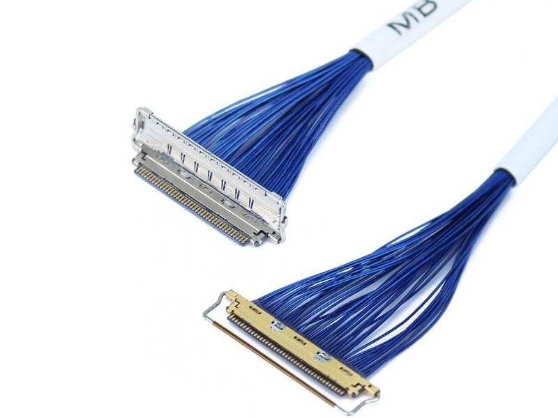
- Superior Signal Integrity (SI): Micro-coax cables feature a central conductor precisely shielded by a dielectric layer and outer conductor (shield), creating a controlled impedance environment (typically 50Ω or custom). This drastically reduces radiation losses, minimizes crosstalk from nearby digital noise, and prevents external interference from disrupting the signal path – essential for clean data transmission at high speeds.
- EMI Containment: The inherent shielding acts like a Faraday cage around the sensitive signal, containing its electromagnetic field and preventing it from interfering with other components (antennas, sensors) and preventing external noise from coupling in. This is vital for passing stringent regulatory certifications (FCC, CE).
- Routing Flexibility: Unlike rigid traces constrained to PCB layers, micro-coax cables are semi-flexible. This allows designers to route signals over or around complex components (large processors, camera modules, batteries), connectors, and areas congested with digital routing, bypassing SI “minefields” on the board itself. Think of routing an MIPI D-PHY signal from a camera sensor module placed away from the main processor block.
- Miniaturization: Ultra-small diameters (often sub-1mm or even down to 0.3mm) enable routing in spaces impossible for standard RF traces or larger coaxial assemblies.
Implementation Challenges on HDI Motherboards
Despite the advantages, integrating micro-coax into densely packed phone motherboards is complex:
- Connector Footprint & Density: Micro-coax connectors (e.g., Hirose U.FL, I-PEX MHF®, JAE SF32) are tiny, but they still require valuable PCB real estate for their pads and keep-out zones. Precisely aligning them with micro-coax landing pads is critical. High connector count demands clever layout strategies.
- Precise Impedance Control: Maintaining controlled impedance doesn’t stop at the cable itself. The transition from the connector solder pads on the PCB through the connector body and onto the cable shield/center conductor must be meticulously designed to minimize impedance mismatches and reflections that degrade signal quality.
- Strain Relief & Reliability: Mobile phones endure drops and flexing. Securing the micro-coax cable near its connection point with strain relief features (clips, anchors, adhesive) prevents connector damage or solder joint fatigue during mechanical stress.
- Placement & Bend Radius: Routing paths must respect the cable’s minimum bend radius (dictated by cable construction and diameter) to avoid kinking, which increases signal loss and risks breaking conductors. Tight bends stress the cable and solder joints. Routes need to be planned carefully to avoid sharp corners or compression.
- EMI at Cutouts/Breaks: Where the cable enters/exits shielded enclosures (e.g., passing through an EMI gasket in a mid-frame), ensuring continuous shield grounding is paramount. Any break in shielding integrity becomes a potential EMI leak point.
- Grounding: The cable’s outer shield must be bonded to the PCB’s RF ground plane at both ends with extremely low inductance paths. Inadequate grounding cripples the shielding effectiveness. This often requires stitching vias very close to the connector ground pads. Creating true “isolation moats” for critical signals is complex.
Mobile Motherboard Design Case Study: High-Res Camera Link
Scenario: Integrating a 108MP camera sensor module located near the top edge of the phone with the image signal processor (ISP) situated centrally on the motherboard. Requires multiple high-speed differential pairs for MIPI C-PHY/D-PHY (> 6 Gbps per lane).
Challenge: The area between the sensor connector and the ISP is densely packed with other components (PMIC, DRAM, antennas) and digital traces. Routing high-frequency MIPI lanes conventionally across this noisy zone risks significant crosstalk and loss, leading to image artifacts or reduced frame rates.
Micro-Coax Solution:
- Signal Selection: The critical high-speed clock and data lanes from the camera module chosen for micro-coax routing, bypassing the noisy central zone. Lower-speed control signals routed conventionally on inner layers.
- Connector Placement: Micro-coax connectors positioned directly adjacent to the camera FPC connector footprint on the PCB edge and very close to the ISP input pins on the main board area. Minimizes the unsupported micro-coax cable length.
- Precision Routing Path:
- Cable path pre-planned in the 3D mechanical CAD model.
- Route goes vertically up from the connector, runs along the shielded inner side surface of the mid-frame/chassis, making gradual bends, before descending vertically down to the ISP connectors.
- Dedicated clearance channels/channels designed into the mid-frame structure to guide and protect the cables.
- Robust Grounding:
- Connectors placed on large, unbroken copper pour areas tied to the primary RF ground plane.
- Stitching via arrays placed immediately around the ground pads of all micro-coax connectors (<0.3mm diameter vias).
- Conductive gaskets used where cables pass through the shield can near the camera module & ISP area.
- Strain Relief:
- Small adhesive anchors securing the cables to the PCB near each connector.
- Cable slack managed with gentle loops where routes change direction to prevent pulling on connectors during assembly/service.
- Manufacturing & Testing:
- Controlled impedance micro-coax cables selected with low loss material (Foamed PE).
- Laser trimming used during module assembly for precise cable termination.
- Significant SI simulation (HFSS/SIwave) performed on the entire path (connector-launch-transition-cable-transition-connector).
- TDR measurements to validate impedance continuity and S-parameter measurements (IL, RL) to ensure signal integrity margins were met post-assembly. Eye diagram validation critical for the target data rate.
Key Takeaways for Success
- Early Integration: Involve mechanical and RF engineers from the beginning of the PCB and industrial design process. Define micro-coax routes in 3D CAD alongside component placement.
- Component Placement Optimization: Place critical ICs (ISP, RF transceiver) and their connectors strategically to minimize micro-coax cable length and routing complexity.
- Grounding is King: Dedicate intense focus to achieving the lowest possible inductance ground connection for micro-coax shields at both ends. Vias, planes, and shielding cans must work together seamlessly.
- Controlled Transitions: The connector-to-PCB and connector-to-cable launch points are high-risk for SI. Model and measure these transitions meticulously.
- Respect Mechanical Constraints: Adhere strictly to minimum bend radii and implement robust strain relief. Factor in thermal expansion/contraction effects.
- Simulate Before Fabricating: Extensive 3D electromagnetic simulation is non-negotiable to predict SI/EMI performance and optimize the design before physical prototypes.
- Material Selection: Choose micro-coax cables with appropriate loss characteristics for your frequency/length requirements and flexible base materials compatible with tight bends (e.g., LCP).
- Prototype & Test Rigorously: Build dedicated micro-coax coupling test structures on early PCBs. Perform TDR, VNA, and high-speed eye diagram tests on the final assembly.